
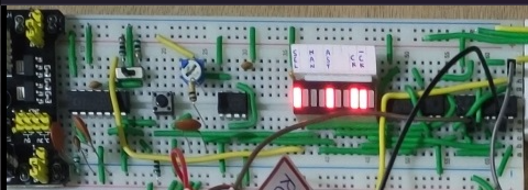
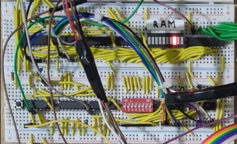
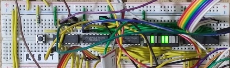
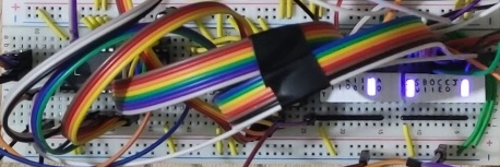
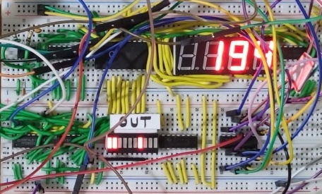
8-BIT BREADBOARD CPU EXECUTING FIBONACCI SEQUENCE PROGRAM
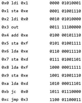
Fibonacci assembly program being executed-
0x0 ldi 0x1
0x1 sta 0xe
0x2 ldi 0x0
0x3 sta 0xf
0x4 out
0x5 lda 0xe
0x6 add 0xf
0x7 sta 0xe
0x8 out
0x9 lda 0xf
0xa add 0xe
0xb jc  0x0
0xc jmp 0x3
0xd hlt
0xe 0x00
0xf 0x00
Check this repository to find sample programs -> https://github.com/YashIndane/8-BIT-TTL-CPU
Story
Usually for beginners or non-technical guys, its hard to understand how a CPU operates and executes the program.
There should be a way to understand on how a basic how individual instructions are executed, which gives a fair bit of idea to us. So I decided to make a CPU on breadboards, using 74 series TTL logic chips which are easy to find.
I decided to make a 8 bit CPU that just runs on some Hz frequency (Not GHZ as we want to see what it does), which will help understanding fundamentals of CPU Operations.
CPU Architecture
This build follows a bus organized Von-Neumann architecture to simplify things as we are literally building a CPU by hands from scratch on breadboards.
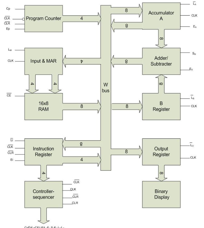
THE BREADBOARD CPU ARCHITECTURE
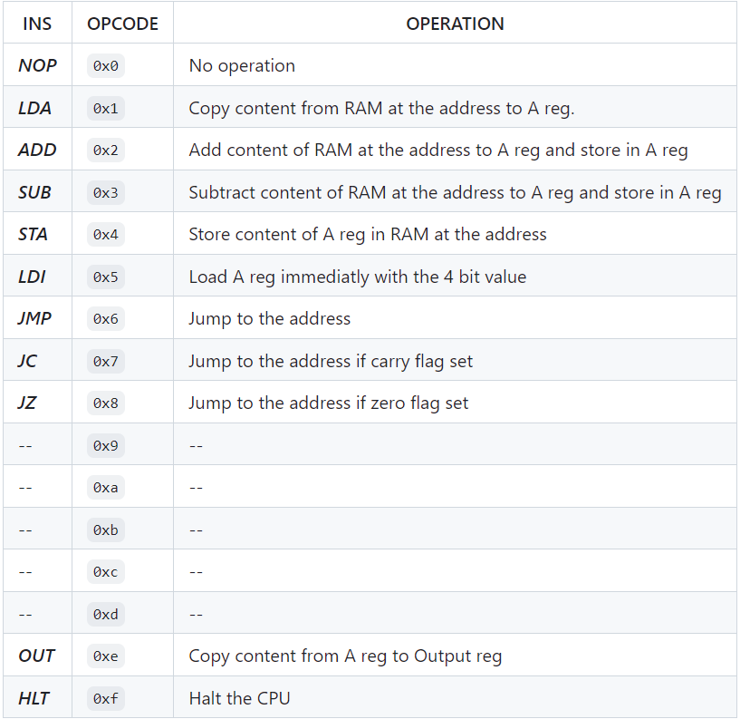
The CPU has its own custom instruction set -
CPU Modules
The CPU is modular and has the following modules -
1.Clock Module - This module generates the clock pulses needed for the CPU to operate using NE555 timers. This is flexible as it also allows to selected between manual or auto pulse. The module uses a NE555 timer to generate the stable pulse to use for auto-mode. A NE556 timer is used to produce a manual pulse to manually step through the execution. Two 74LS00 ICs are used to incorporate the logic for switching between modes and use the HLT signal as well.
| Control Signal | Description |
| HLT (active-high) | This signal is used to halt the CPU |
2. Program Counter Module - This module uses a 74LS161 4-bit counter chip which can also be made to load a desired value in case of a JMP instruction. It holds the address of next instruction to be fetched. This increments itself after the last instruction fetch cycle, and points to next instruction address.
| Control Signals | Description |
| CO (active-low) | Counter Out signal, is used to place the value of Program Counter on Bus |
| J (active-low) | Jump signal updates the Program Counter with desired Jump address |
| CE (active-high) | Count enable just increments the Program Counter value after the instruction fetch cycle |
3. RAM Module - This uses two 74LS189 RAM ICs to get a 16 by 8 bit word RAM. This is a 16 Byte RAM that holds the assembly code to be executed. This chip has inverted outputs, so 74LS04 inverter chips has to be used to re-inverts those and feed it to 74LS245 Octal Bus Trans receiver chip, to connect the module to the BUS.
| Control Signals | Description |
| RO (active-low) | RAM out signal is used to put the contents of the RAM on the BUS |
4. ALU Module - This uses two 74LS283 Full adders to do the 8 bit calculations as needed. The module uses 2's complement method in order to execute subtraction instruction. 74LS86 XOR chip is used to invert the contents of B register and also add 1 to ALU, to get the 2's complement of the B register and adding it with A register, which is equivalent to subtraction. It also uses 74LS245 Bus trans-receiver to connect itself to the BUS.
| Control Signals | Description |
| SO (active-low) | Sum out signals puts the result of ALU on the BUS |
| SUB (active-high) | Subtract signal is used to perform subtraction operation |
5. A and B register - This are two 8 bit registers build using four 74LS173 4 bit registers. A register acts as the accumulator. It also uses 74LS245 Bus trans-receiver to connect itself to the BUS.
| Control Signals | Description |
| LOAD (active-low) | LOAD signal will update the content of register with the value on BUS |
| OUT (active-low) | OUT signals will place the value in register on the BUS |
6. Instruction Register - This 8 bit register holds the current instruction that is being executed. Its build using 74LS173 ICs. It also uses 74LS245 Bus trans-receiver to connect itself to the BUS.
| Control Signals | Description |
| II (active-low) | Instruction register IN signal will update the value of Instruction Register with value on BUS |
| IO (active-low) | Instruction register OUT signal will place the value in it on the BUS |
7. Flags Register - Its a 2 bit register, that holds value for Zero and Carry Flag. The status of the flags register is considered while executing conditional jumps like JZ AND JC.
| Control Signals | Description |
| FI (active-low) | Flags IN signal will update value of Flags Register with status of ALU result |
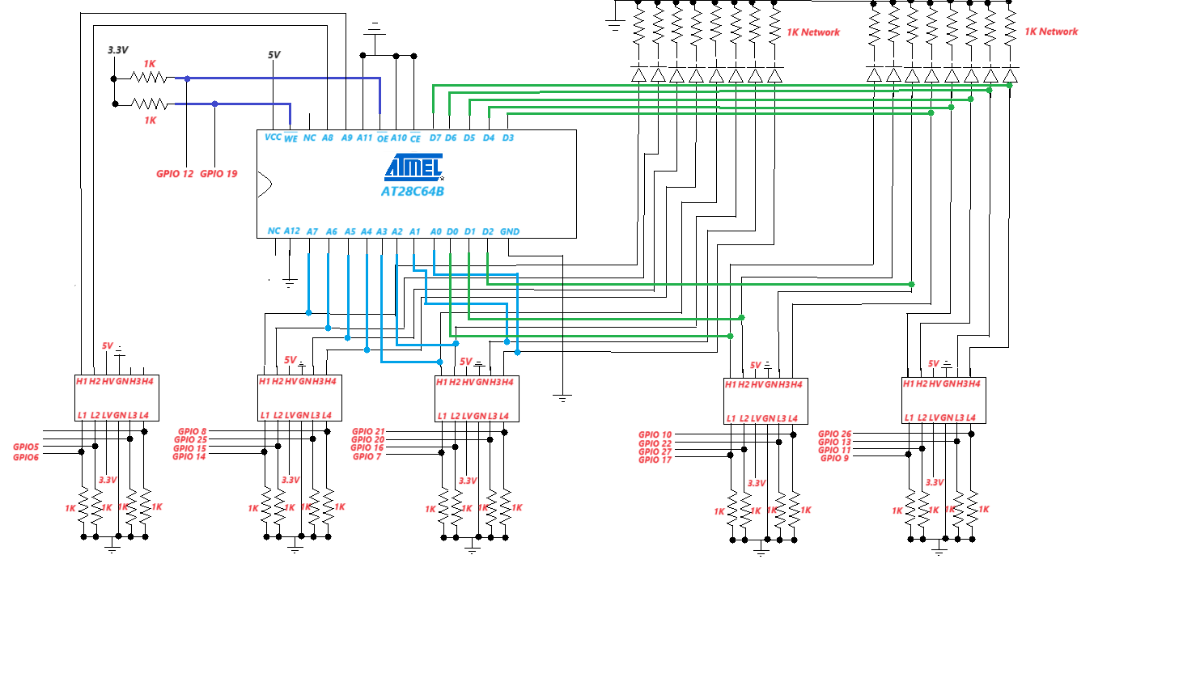
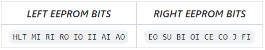
8. Instruction Decoder - This is actually the most important module as it decodes the instructions and generates the control signals to get the instruction executed. It sets the control signals on the falling edge of the clock. The CPU has total 16 control signals, and it uses two ATMEL 28C64B Parallel EEPROMs to generate those control signals.
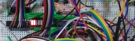
9. Output Display - This uses a seven segment display to show the output of programs. It displays values from 0 to 255 as its a 8 bit CPU. It uses ATMEL 28C64B and multiplexing technique to generate the required segments according to the 8 bit number.
Programming the CPU
To program the CPU we need to enter the machine code generated using DIP switches. A python script helps to generate machine code from assembly code. Writing the machine code from assembly code manually is a tedious task. To make life easy, use the assembler.py script to do the same job quickly.
python assembler.py --asmfile="<ASSEMBLY-FILE>"
This will output binary address and data values, which we can then manually enter to CPU's RAM using DIP switches. Sample output -
Working
First the machine code is programmed in the RAM (74LS189) to be executed, using the program mode. Then we switch to the run mode and set the clock speed, and run the CPU.
In the instruction fetch cycle, the program counter value is copied to the memory address register, which makes it point the RAM to the required memory location, from where to start to execute the program. The instruction is copied to the instruction register, which changes the state of the control EEPROMs to send the appropriate control signals to execute the instruction. This keeps on repeating until the CPU reaches the HALT instruction.
Programming the Instruction Decoder & Output Display Module EEPROMs
Schematic for programming the EEPROM with flags-
The instruction Microcode Word -
The individual instruction and its micro-code decoding pattern is saved in a JSON file -
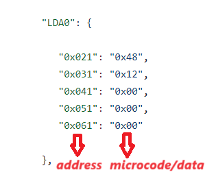
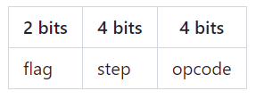
For example, the LDA0 denotes LDA instruction with no flags set condition. The address & microcode/operand values are encoded in hex format for easy representation. This JSON file with all the instructions encoded in hex format are fed to a python script to burn it to the EEPROM using a Raspberry Pi Zero 2W. The address bit field is split as follows -
Cleaning the EEPROM -
$ sudo python3 eeprom_cleaner.py
Bulk writing -
$ sudo python3 eeprom_bulk_write.py --eefile="<JSON-FILE>"
Please check this link on how to program the instruction decoder EEPROMs and the Output display EEPROMs ->
https://github.com/YashIndane/rpi-eeprom-programmer
Applications
This Project is mainly built for educational purposes, which can be used by school/college students to understand various components of a CPU and understand Assembly language. This project gives a deep insight of the inner workings of a CPU like fetch cycle, register to register transfers etc to the user, in a simple visual way. This project can be further expanded to visualize more complex processor designs.
Future Developments
- Adding a LCD display to display the output of the program
- Using better approach to burn the assembly code to RAM
- Using a pipelined CPU approach to run more complex instructions
Conclusion
This project is a working demonstration of a complete CPU which can be used to study CPU Operations and Digital System Design.
Thank You!