
What is a MOSFET?
An integrated circuit IC or electronic device that uses a lot of transistors is called a MOSFET (Metal-Oxide-Semiconductor Field-Effect Transistor). There are two potential applications for this three-terminal device: switching and amplifier. A thin oxide insulating layer, usually silicon dioxide, separates a MOSFET's metal gate electrode from its semiconductor channel. The current flowing through the channel is controlled by the voltage that is provided to the gate terminal. MOSFETs are well known for their quick switching speeds, low power consumption, and ability to tolerate large currents and voltages. They are widely used in voltage regulator, power amplifier, and digital logic circuits. Ersa Electronics provides all kinds of transistors like BJT transistors, FETs, MOSFETs, IGBTs, and JFETs.
MOSFET Pinout
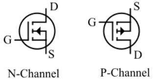
Pinout of a MOSFET is as follows:
Gate (G): The gate is the control terminal of a MOSFET. By supplying a voltage, the gate controls the amount of current that flows between the source and drain terminals.
Source (S): The source of a MOSFET is the terminal through which current enters it.
Drain (D): The MOSFET terminal where the device's current exits is referred to as the drain.
Bulk (B): The bulk is the MOSFET substrate. It is connected to the source terminal in the majority of programs.
Types of MOSFET
N-channel MOSFET: The substrate of this kind of MOSFET is made of an n-type semiconductor material. The most popular kind of MOSFETs are N-channel MOSFETs. They are utilized in many different applications, such as analog circuits, microprocessors, and power electronics.
P-channel MOSFET: The substrate of this kind of MOSFET is made of p-type semiconductor material. Although they are not as widely used as n-channel MOSFETs, P-channel MOSFETs are nonetheless employed in many different applications. They are frequently utilized in complementary circuits, which combine n- and p-channel MOSFETs for improved performance.
DMOSFET: Double-Diffused MOSFET is what this acronym stands for. Because of its design, this kind of MOSFET performs better at high voltages and currents. In power electronics applications,
What is an IGBT?
Insulated Gate Bipolar Transistor is referred to as IGBT. It is a three-terminal semiconductor device, similar to a MOSFET, that combines the high input impedance of a MOSFET with the high current-handling capability of a bipolar transistor. IGBTs also have a collector (C), an emitter (E), and a gate. The gate controls conduction between the emitter and collector, therefore controlling current flow.
IGBT Pinout
.jpeg)
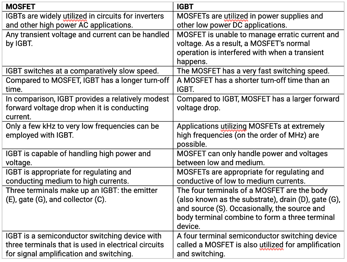
MOSFET vs. IGBT
How to Test a MOSFET?
- Disconnect the MOSFET from any power supply or circuitry to guarantee safety.
- On your multimeter, choose the resistance or diode test mode.
- Ascertain the drain (D), source (S), and gate (G) MOSFET terminals. Refer to the datasheet or the MOSFET's markings for identification.
- Connect the positive (red) probe of the multimeter to the gate terminal (G) and the negative (black) probe to the source terminal (S).
- Examine the multimeter's reading. If the MOSFET is enhancement-mode type, the multimeter should show an open circuit or very high resistance. If the multimeter is of the depletion-mode type, it can show a closed circuit or low resistance.
- Reverse the probe connections such that the source terminal (S) is connected to the positive (red) probe and the gate terminal (G) is connected to the negative (black) probe.
- Examine the multimeter reading once more. An enhancement-mode MOSFET should keep displaying an open circuit or high resistance. A depletion-mode MOSFET's measurement may change, indicating a low resistance or a closed circuit.
- If the MOSFET passes these tests, it can subsequently be checked at the drain-to-source junction. Attach the red positive probe to the drain terminal (D) and the black negative probe to the source terminal (S).
- Analyze the multimeter's reading. When the MOSFET is functioning properly, its drain-to-source termination should resemble a diode. The resistance for the forward bias should be low, whereas the resistance for the reverse bias would be high.
- Change the probe connections to the correct ones: negative (black) on the drain terminal (D) and positive (red) on the source terminal (S). Do the exam again. If the MOSFET behaves strangely or doesn't pass any of these tests, replace it right once to rule out a problem.
How to Test a IGBT?
- Using the diode scale with a digital ohmmeter.
- Determine the resistance between E2 and C2/E1.
- Determine the resistance between C1/E1 and C2/C1.
- Using the diode scale with a digital ohmmeter.
- Feel the - (black) meter lead at E1 and the + (red) meter lead at G1.
- Feel the - (black) meter lead to E2 and the + (red) meter lead to G2.
- Determine the resistance between C2/E1 and C1. Low resistance (about a diode drop) should be read. The reading on the reverse meter leads should be the same.
- Determine the resistance between C2/E1 and E2. Low resistance (about a diode drop) should be read. The reading on the reverse meter leads should be the same.
- using the diode scale with an ohmmeter.
- Touch E1's (+) red meter lead and G1's (-) black meter lead.
- Feel the - (black) meter lead to G2 and the + (red) meter lead to E2.
- Assess the resistance between C1/- and C2/E1 (+). Low resistance should be read (same as in step 2c.). Meter leads in reverse. See endless opposition.
- Determine the resistance between E2 (+) and C2/E1 (-). Low resistance should be read (same as in step 2d.). Meter leads in reverse. See endless opposition.
How does a IGBT work?
MOSFET Turned Off: A MOSFET is turned off when the gate voltage is low. This indicates that no current is flowing through the MOSFET and that there is a high resistance between the gate and the source.
MOSFET Turned On: The MOSFET turns on when the gate voltage reaches a certain level. This indicates that current can pass through the MOSFET and that there is a large drop in resistance between the gate and the source.
Bipolar Transistor Amplifier: Carriers can move from the emitter to the collector when the MOSFET is turned on. The bipolar transistor can then handle higher voltages and currents thanks to the flow of these carriers through it, which amplifies the current.
Conclusion of MOSFET vs. IGBT
When compared to alternative power switching components, such as the conventional MOSFET option, an IGBT offers numerous advantages. IGBTs, with their intrinsic reduced voltage drop, will boost the efficiency in most applications with a supply voltage over 300 V, especially when running at high temperatures. This simplifies the thermal design and lowers the need for a heat sink. Because the semiconductor current channel in IGBTs is shorter and has a higher current density, the thermal impedance is decreased.
IGBTs work especially well in high current/high voltage systems operating at frequencies of 100 kHz or below. This is because, as compared to MOSFETs with comparable ratings, the IGBT has reduced switching and conduction losses. In IGBT applications, overload durability is increased and snubbers are either unnecessary or need to be reduced. Because of the softer waveforms during IGBT switching, the application produces less EMI.