Introduction
- PIC18F4550 has an inbuilt CCP module which has Capture, Compare, and PWM mode for various applications.
- CCP in Compare mode is used to generate a waveform of various duty cycles like PWM and also used to trigger an event when the pre-determined time expires.
- Also, it is used to generate specific time delay.
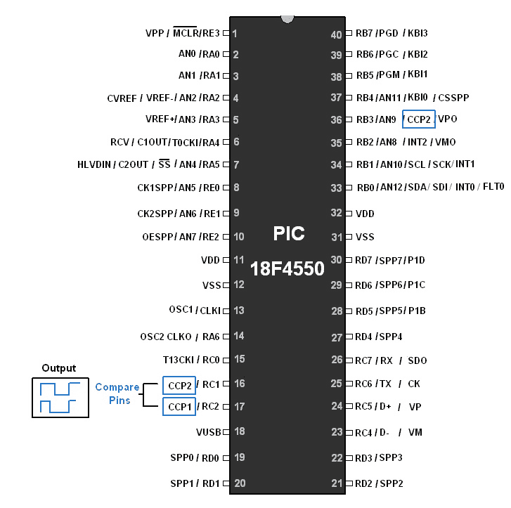
- PIC18F4550 has 2 in-built CCP modules i.e. CCP1 and CCP2.
- Output (e.g. Waveform generation) of CCP2 and CCP1 in compare mode is generated on two pins i.e. RC1 and RC2 respectively.
CCP module Pins

CCPR1 Register
CCP module has 16-bit register CCPR1 [CCPR1H (8-bit): CCPR1L (8-bit)] given below in which count is loaded to compare.

The compare mode of the CCP module is selected using bits in the CCP1CON Register.
Only Timer1 and Timer3 can be used for Compare mode in PIC18F4550.
Operation of Compare mode

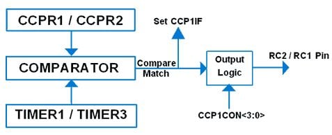
In compare mode, the 16-bit CCPR1 register value is constantly compared against either the TMR1 or the TMR3 register pair value shown in the figure given below.
When a match occurs between the CCPR1 Register value and Timer value, the CCP1IF interrupt flag is generated and one of the following actions may occur on the associated RC2 pin:
- Toggle output on the RC2 pin.
- RC2 pin drives to a High level.
- RC2 pin drives to a low level.
- Generate software interrupt
- Generate a special trigger event.
Now, what output logic will generate when a compare match occurs depend on the CCP1CON register.
CCP1CON Register: CCP1 Control Register
DC1B1:DC1B0:
Used for PWM mode.
CCP1M3:CCP1M0: CCP1 module mode select bit
These bits decide which action takes on compare match.
0010 = Toggle output on match
1000 = Initialize CCP1 pin low, on compare match this pin is set to high.
1001 = Initialize CCP1 pin high, on compare match this pin is set to low.
1010 = On compare match generates software interrupt.
1011 = On compare match trigger special event, reset the timer, start ADC conversion.
So Configure compare mode as per application using CCP1CON Register.
Other combinations are used for Capture and PWM mode.
Interrupt on Match
Also, remember that after every compare match between CCPR1 and Timer1/Timer3 CCP1IF interrupt flag is set.
This flag is located at PIR1<bit2> Register.
Also, note that the T3CON register is used to select Timer1 or Timer3 for compare mode.
T3CON Register: Timer3 Control Register

T3CCP2:T3CCP1: Used to select Timer for Compare mode operation.
00 = Timer1 for both CCP module
01 = Timer1 for CCP1 module
Timer3 for CCP2 module
1x = Timer3 for both CCP module
Calculation
Now How to calculate Count for CCPR1?
The following figure illustrates steps to calculate count for the desired delay which to be load into CCPR1 Register.

Steps for Programming
- Set the CCP1 pin as an output.
- Configure T3CON Register for Timer1 or Timer 3
- If Timer1 is used then configure T1CON Register also.
- Configure CCP1CON Register for compare mode.
- Load desired count in CCPR1 (CCPR1H: CCPR1L) Register.
- Also, initialize TMR1 or TMR3 register value.
- Start Timer
- Wait for CCP1IF (PIR1<2>) interrupt flag to set.
- Then Clear Timer Register (TMR1 or TMR3).
- Jump to step 3.
Application 1
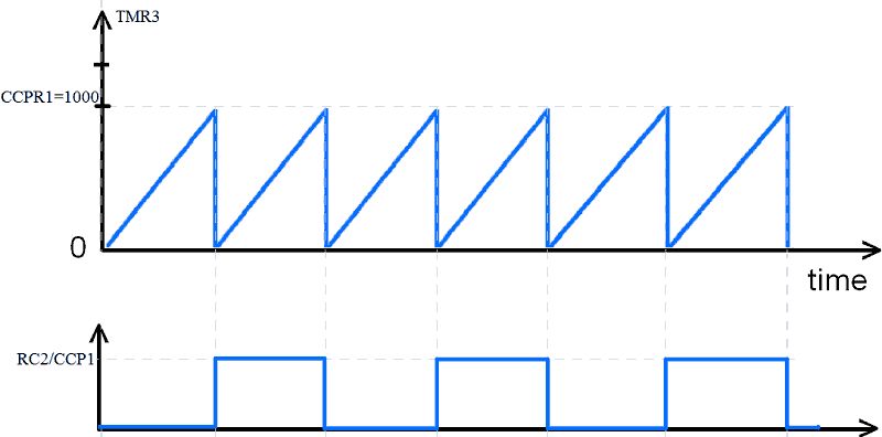
Here let’s generate a square wave of 1 kHz having a 50% duty cycle.
For 50% Duty Cycle
Assume Oscillator frequency = 8MHz
Period of waveform = 1ms (1 KHz given)
So Instruction Cycle = 1/ (FOSC/4) = 1/ (8MHz/4) = 0.5 us
That means Timer will increment its count continuously after each 0.5us delay.
Here I used the Timer3 register.
Now calculate CCPR1 count.
For 50% Duty Cycle – ON time=OFF time=0.5ms
0.5ms/0.5us = 1000 i.e. 0x03E8
CCPR1 = 0x03E8
PIC18F4550 1kHz 50% duty cycle Square wave generation program
/*
 * Generate waveform of 1KHz having 50% duty cycle
 * https://www.electronicwings.com
 */

#include "osc.h"
#include <p18f4550.h>

void main()
{
    OSCCON=0x72;	/* Configure internal clock at 8MHz */
    TRISCbits.TRISC2=0;	/* Configure RC2 pin as output */
    CCP1CON=0x02;	/* Module is configured for compare mode and is set up so that upon a compare match of CCPR1 and TMR3, RC2 is driven low*/
    PIR1bits.CCP1IF=0;	/* Clear interrupt flag*/
    TMR3=0;		/* Clear Timer3 Register*/
    T3CON=0xC0;		/* Timer3 used for compare mode with TMR3 register in 16-bit format*/
    CCPR1=1000;		/* Load a count for generating 1khz*/
    T3CONbits.TMR3ON=1;	/* Turn On Timer3*/
    while (1)
    {
      /* Wait for CCP Interrupt flag to set, it is set on compare match between CCPR1 and TMR3*/
      while(PIR1bits.CCP1IF==0);
      PIR1bits.CCP1IF=0;/* Clear interrupt flag */
      TMR3=0;
    }
}
Output

Application 2
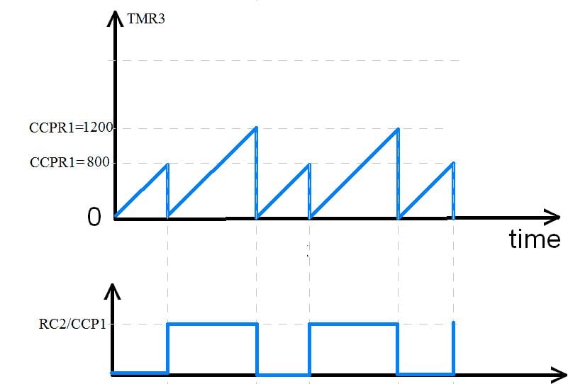
Now generate another 1KHz waveform with a 40% duty cycle.
For 40% Duty Cycle,
ON time=0.4ms, OFF time=0.6ms
0.4ms/0.5us = 800 i.e. 0x0320
0.6ms/0.5us = 1200 i.e. 0x04B0
Load these values into CCPR1 Register
PIC18F4550 1kHz 40% duty cycle Square wave generation program
/*
* Generate waveform of 1KHz having 40% duty cycle
* https://www.electronicwings.com
*/

#include "osc.h"
#include <p18f4550.h>

void main()
{
    OSCCON=0x72;	/* Configure internal clock at 8MHz */
    TRISCbits.TRISC2=0;	/* Configure RC2 pin as output. */
    CCP1CON=9;		/* Module is configured for compare mode and is set up so that upon a compare match of CCPR1 and TMR3, RC2 is driven high*/
    PIR1bits.CCP1IF=0;
    TMR3=0;
    T3CON=0xC0;		/* Timer3 used for capture mode with TMR3 register in 16-bit format*/
    CCPR1=0x320;	/* Load a count for generating 0.4ms*/
    T3CONbits.TMR3ON=1;	/* Turn On Timer3*/
    while(1)
    {
       /* Wait for CCP Interrupt flag to set, it is set on compare match between CCPR1 and TMR3*/
        while(PIR1bits.CCP1IF==0);
        PIR1bits.CCP1IF=0;	/* Clear interrupt flag*/
        TMR3=0;			/* Clear Timer3 Register*/
        CCP1CON=8;		/* CCP1 module is configured for compare mode and is set up so that upon a compare match of CCPR1 and TMR3, RC2 is driven low*/
        CCPR1=0x04B0;		/* Load count for generating 0.6ms */
        while(PIR1bits.CCP1IF==0);
        PIR1bits.CCP1IF=0;
        TMR3=0;			/* Clear Timer3 Register*/
        CCP1CON=9;
        CCPR1=0x0320;		/* Load count for generating 0.4ms */

    }
}
Output

Video
Components Used |
||
|---|---|---|
| PIC18f4550 PIC18f4550 |
X 1 | |
| PICKit 4 MPLAB PICKit 4 MPLAB |
X 1 | |